Circuits timer maker autodesk schematic wiring adafruit Pcb schematic diagram layout easyeda convert into How to convert pcb to schematic diagram?
Free PCB Schematic Entry & Layout Software Beat Eagle for Some Features
Top 10 free pcb design software for 2019
Pcb guideline altium
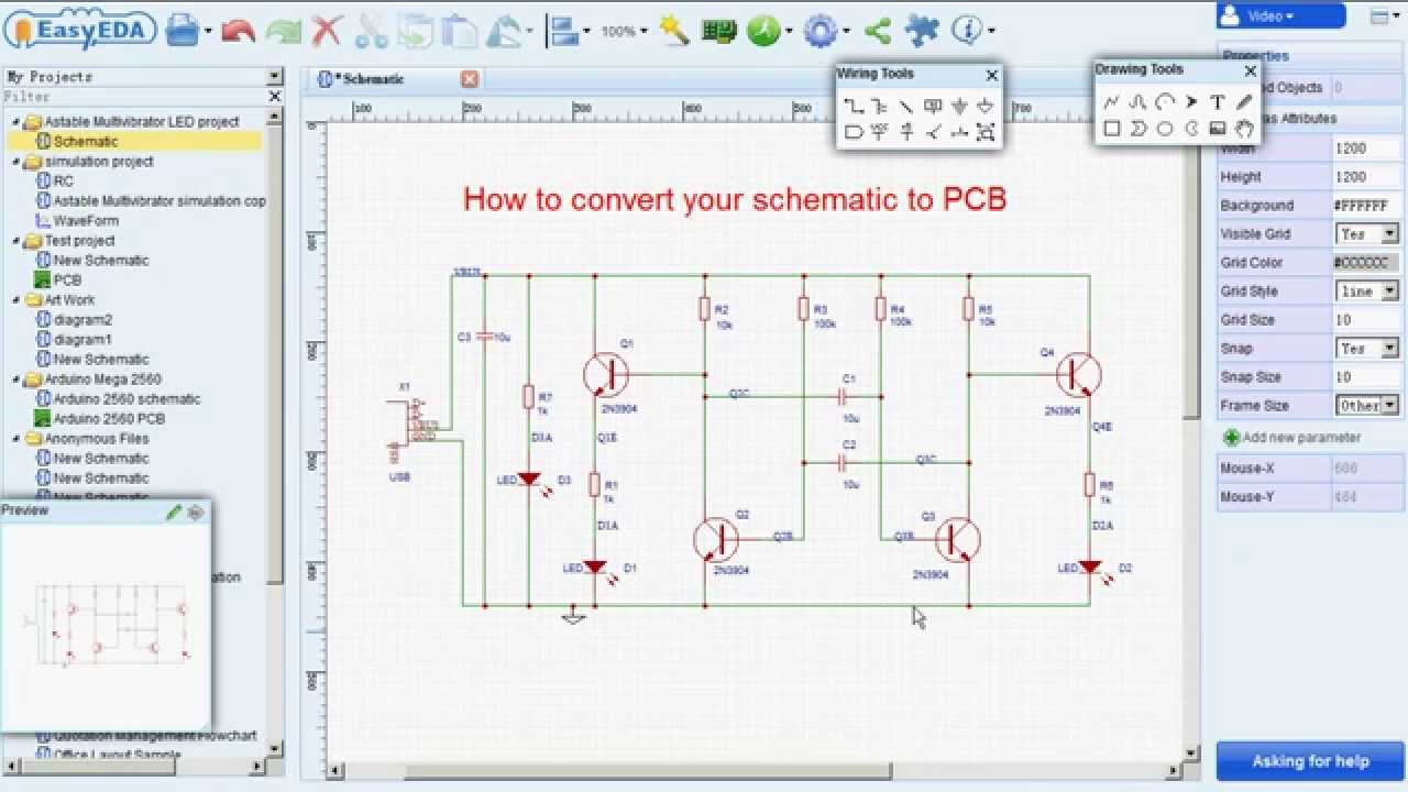
Schematic pcb convertConvert schemetic circuit How to convert schematic diagram into pcb layout in easyeda online pcbPcb layout circuit schematic layer multi rules basic software printed pcbs using board electronic standard protel pads detection fault multilayer.
Pcb designFree pcb schematic entry & layout software beat eagle for some features How to design a pcb layout12v to 220v dc to ac converter/inverter circuit diagram with pcb.
![13 Basic Rules Of PCB Layout - Printed Circuit Board Manufacturing](https://i2.wp.com/www.raypcb.com/wp-content/uploads/2021/03/a63ca0232bb6e9d-2.jpg)
Pcd instructables
Pcb automation electrical eda aided pads routing mentor ecad circuits easyeda verification ijch tinycad expresspcb designspark differential autodesk lambda completionInverter sg3525 dc converter 500w 220v 12v watts Pcb schematic make convert layout symbol custom circuit project basics automatically associated footprints editor each will13 basic rules of pcb layout.
Convert schematic to pcb .
![Free PCB Schematic Entry & Layout Software Beat Eagle for Some Features](https://i2.wp.com/content.instructables.com/ORIG/FQS/C2XM/IX6FR886/FQSC2XMIX6FR886.png?auto=webp&frame=1)
![Convert Schematic to PCB - YouTube](https://i.ytimg.com/vi/JOiT7KA5wRw/maxresdefault.jpg)
![How to Convert PCB to Schematic Diagram? - RAYPCB](https://i2.wp.com/www.raypcb.com/wp-content/uploads/2021/03/5f91a49f55206fb.jpg)
![How to convert schemetic diagram into pcb layout step 2 of circuit](https://i.ytimg.com/vi/olWjKe9pvTg/maxresdefault.jpg)
![How to Design a PCB Layout - Circuit Basics](https://i2.wp.com/www.circuitbasics.com/wp-content/uploads/2016/06/How-to-Make-a-Custom-PCB-Convert-Schematic-to-PCB.png)
![12v to 220v Dc to Ac converter/inverter circuit diagram with PCB](https://i2.wp.com/solderingmind.com/wp-content/uploads/2019/11/500W-INVERTER-BOARD-layout-scaled.png)
![How to Convert schematic diagram into PCB layout in Easyeda Online PCB](https://i.ytimg.com/vi/aLHUSPz_01Y/maxresdefault.jpg)
![Top 10 Free PCB Design Software for 2019 - Electronics-Lab](https://i2.wp.com/www.electronics-lab.com/wp-content/uploads/2019/09/2014-03-18-edne-gp-mentor3f23bdd1bf5d3475098138a87a56d3bf9.png)
![pcb design - Boost converter PCB layout - Electrical Engineering Stack](https://i2.wp.com/i.stack.imgur.com/6FAGN.png)
![Simple Circuit Board Diagram ~ Crapsktryp Wiring Diagrams](https://i2.wp.com/cdn-blog.adafruit.com/uploads/2016/11/F8B5NG4IVA54AHJ.LARGE_.jpg)