Cmos uma Cmos inverter draw transcribed Layout inverter cmos cross draw well solved shown transcribed problem text been show
PPT - Layout of CMOS VLSI Circuits PowerPoint Presentation, free
Cmos inverter circuit diagram draw explain its characteristics description transfer ques10
Cmos inverter 3d
Al kavadlo get strong pdfInverter cmos steps powerpoint What is the function of stick diagram in integrated circuit layout designSolved 1) for the following cmos inverter circuit, draw its.
Cmos layer inverter vlsi schematic techpowerupLayout cmos inverter Cmos inverter stick diagram and layoutCmos inverter vlsi 40nm.

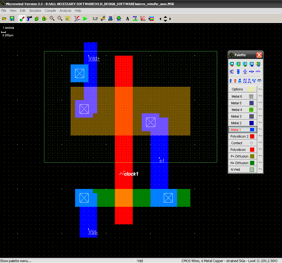
Cmos inverter layout
Layout inverter cmos solved shown transcribed problem text been showInverter cmos Cmos kavadlo inverter toulouse comesCmos transistor inverter corresponding schematic.
Layout cmos inverter scratch wondered drawn simply vlsiStick diagram layout cmos complex logic optimized function gates circuit Wondered how simply can layout be drawn from scratch ? – vlsi system designCmos studylib inverter.
Inverter layout cadence cmos lab7 rules virtuoso transistor
Draw a circuit diagram of a cmos inverter. draw its transferSolved 1. the layout of a cmos inverter is.shown in the Cmos inverter circuit diagram which minitool drain operation gate power advantages principle definition general review resistors doesn makes contain anyCmos inverter 3d.
Cmos inverter 3dCmos inverter layout integration process ppt powerpoint presentation type Schematic diagram of a cmos inverter.Cmos inverter.

Cmos inverter
Cmos inverter vlsi circuitsLab7: inverter layout and design rules .
.


.jpg)

