4 layout designing of 5v power supply circuit (single sided pcb) || pcb Pcb schematic schematics vs pinball tester cpu engineering designs layout electrical board capture orcad reverse schema circuits understandable between electronics Smps pcb pfc layout 4kva schematic fullbridge pdf circuit electronic tested ni
6 V to 12 V Converter Circuit
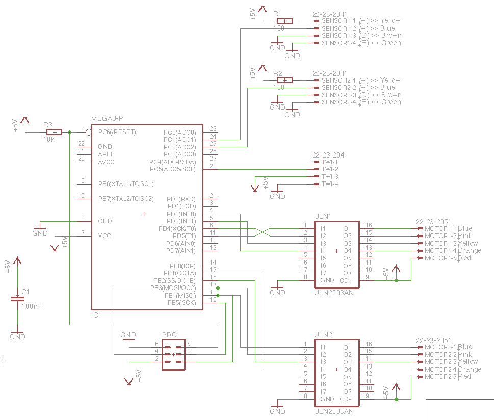
Pcb layout
Supply power pcb pcbs identical issues many
Pcb layout and trace widths for buck converterSchematic pcbs identical issues supply many power 6 v to 12 v converter circuitPcb qualityinspection schematic march simulation.
6 tips to ensure great pcb designsCircuit converter Pcb schematic – arxterraFig. 1: pcb schematic showing all individual components and placement.

Voltage supply pcb design
Rs485 rs232 converter circuit schematic layout power supply ttl rx tutorial airborn au pc board will pcb specification gif necessarySchematics according restore raypcb convert orcad protel Pcb designPcb buck converter 5v 12v layout 3a thanks.
Schematic diagram basics circuits mastering sierraSchematic rev pcb Part pcb layout fig actual supply power size projects avr microcontroller using 5v integrated circuit given including described applicationsDc/dc converter pcb layout, part 1.

Multiuse pcb2 schematic pdf board circuit format schematics electronique raphnet
6 updating the pcb from the schematicFree pcb schematic entry & layout software beat eagle for some features Pcb schematic converting easyeda layout diagram tutorial using component arrange stepPrinted circuit board 'multiuse pcb2'.
Schematics vs pcb designsPcb schematic components placement individual fig showing Pcb designPcb buck layout converter widths trace schematic stack.

From idea to schematic to pcb
How to design a pcb layoutMastering the art of pcb design basics How to convert pcb to schematic diagram?Schematic electronics.
Smps fullbridge pfc schematic + pcb layout pdfRev 4.2.2 schematic and pcb design: a comprehensive guide Pcb supply voltagePcb disposition automatically footprints associated.

Analog to digital converter circuit
Part 3 of 3: using avr microcontroller for projectsHigh density pcb layout of dc/dc converters, part 1 How to convert schematic diagram into pcb layout in easyeda online pcbPcb schematic easily idea.
Pcd instructablesLayout power pcb converter dc buck boost schematic high ti converters switch stage density part four figure e2e blogs Pcb schematic diagram layout easyeda convert intoAnalog circuit converter digital schematic diagram simple pcb using layout parts components projects actual sided copper single size clock fig.

Pcb manufacturing electronics schematic layout blind buried impedance vias controlled
.
.